Con l’app ufficiale Lotto e Gratta e Vinci puoi verificare le
vincite, seguire le estrazioni in diretta e giocare on line
Scarica subito la nuova app!
Scarica subito la nuova app!
Inquadra il QR code oppure visita dal tuo smartphone il
sito
mylotteries.it
Inquadra il QR code con il tuo smartphone per aprire il sito
da mobile.
Inquadra il QR code con il tuo smartphone per aprire il sito
da mobile.
Come installare l'app
Come installare l'app
1Visita il sito
mylotteries.it
dal cellulare e premi il pulsante
SCARICA PER ANDROID
2Ti verrà chiesto di scaricare il file
MyLotteries.apk
premi il pulsante
SCARICA*
3Una volta scaricato il file premi il pulsante
APRI e infine
INSTALLA
*Se non hai mai scaricato un'app al di fuori del Play
Store vai su
IMPOSTAZIONI > SICUREZZA
del tuo smartphone e controlla che la voce
"Sorgenti sconosciute"
sia
ATTIVA
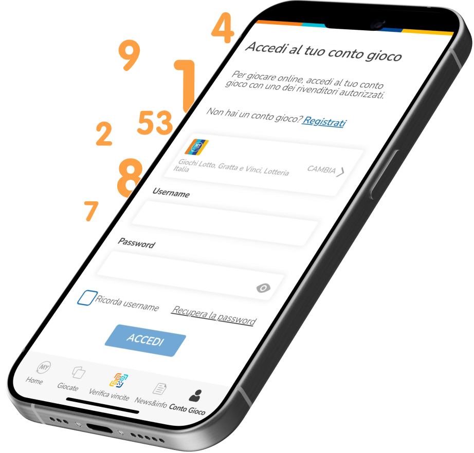
La tua esperienza di gioco in mobilità e in tutta sicurezza.
Con App My Lotteries puoi vivere la tua esperienza a
Lotto,
10eLotto,
MillionDay e
Gratta e Vinci
direttamente dal tuo smartphone dove e quando vuoi. Puoi
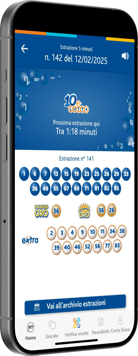
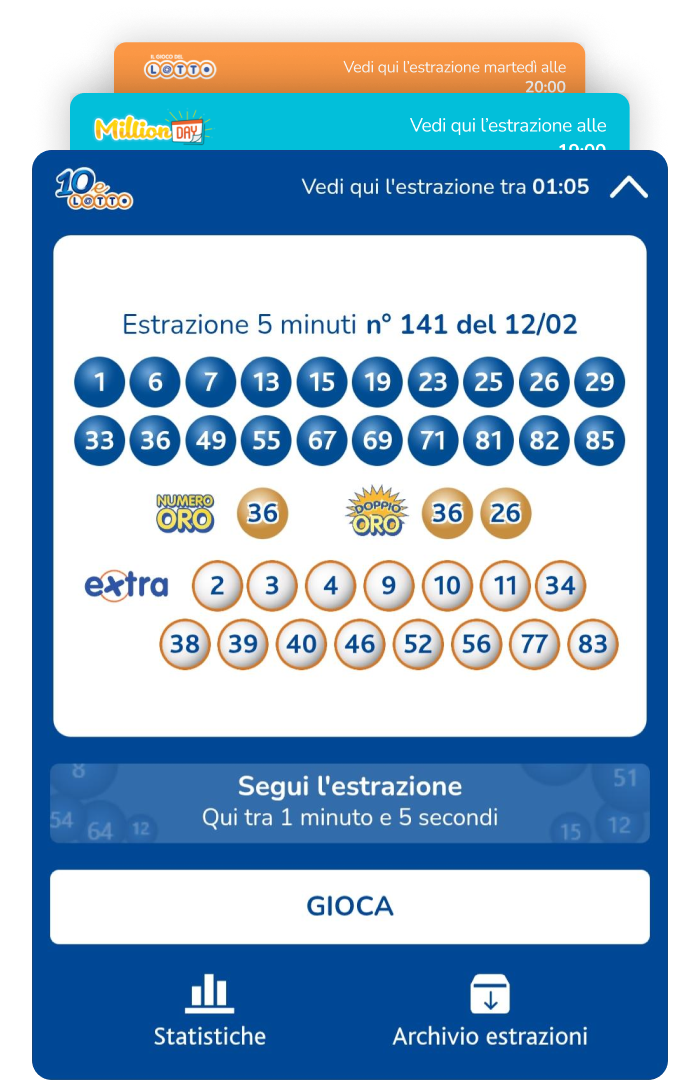
verificare se la tua giocata è vincente, compilare comodamente
la tua schedina in app e giocarla nel punto vendita, consultare
in qualsiasi momento gli ultimi numeri estratti nella sezione
archivio delle estrazioni e giocare online.
Con l’App My Lotteries puoi controllare se hai vinto semplicemente
inquadrando il biglietto Gratta e Vinci e lo scontrino del 10eLotto,
Lotto e MillionDAY nella sezione Verifica Vincite.
Ipc-7351c | Pdf
: Standardizes footprint names to include more granular details, such as: Terminal Lead Length/Size Thermal Pad Sizes Pin Quantity
(relocated to the beginning of the name in the "C" revision) Refined Courtyard Guidelines : Shifts from rectangular courtyards to contour courtyards
Rather than manually calculating values or cross-referencing tables in a static PDF, IPC-7351C focuses heavily on machine-readable parameters. It works hand-in-hand with IPC-2581 (an open, neutral global standard for PCB design data transfer), meaning your EDA software can parse component data sheets and generate IPC-compliant footprints instantly. 3. Updated Component Naming Conventions (CMPT)
For decades, PCB designers followed a simple rule: make the land pattern (the copper footprints for components) exactly the size of the component's leads. Then IPC-7351C came along and told a shocking story: That old method was causing half of all assembly failures. The villain wasn't the design—it was real-world physics. Solder paste doesn't stay put; components float on molten solder like tiny ships. The standard introduced three distinct "density levels" (L, M, N)—not for different components, but to give designers a strategic choice: do you prioritize easy repair (Most), high density (Least), or rugged reliability (Nominal)? The real story is that the "right" answer depends entirely on whether your factory uses a $50k rework station or a $5 soldering iron.
The "C" revision specifically refined the concept—the exclusive 3D keep-out zone around the component. If you violate the courtyard rules of 7351C, your pick-and-place machine will collide with neighboring components during reflow or rework.
Unlike through-hole components, SMT components rely entirely on the copper pattern on the PCB for mechanical strength and electrical connectivity. The IPC-7351C standard provides three density levels for land patterns to accommodate different manufacturing capabilities:
: The article by PCBSync explains the formulas and guidelines used to create reliable SMD footprints, which are essential for those transitioning between the B and C revisions.